At 200 times stronger than steel, graphene has been hailed as a potential material of the future since its discovery in 2004. The ultrathin carbon material is a very strong electrical and thermal conductor, making it an ideal ingredient to enhance semiconductor chips found in many electrical devices.
But while graphene-based research has been fast-tracked, the nanomaterial has hit a few roadblocks. In particular, manufacturers have not been able to create large, industrially relevant amounts of the material.
However, new research from the laboratory of Nai-Chang Yeh, a physics professor at the California Institute of Technology (Caltech) (Pasadena, California, USA), could change that.
Two Studies
In two recent studies, Caltech researchers have demonstrated that graphene can greatly improve electrical circuits required for wearable and flexible electronics such as smart health patches, bendable smartphones, helmets, large folding display screens, and more.
In one study, published in ACS Applied Materials & Interfaces,1 the researchers grew graphene directly onto thin two-dimensional copper lines commonly used in electronics. The results showed that the graphene not only improved the lines’ conducting properties, but it also protected the copper-based structures from usual wear and tear.
For instance, they showed that graphene-coated copper structures could be folded 200,000 times without damage, as compared to the original copper structures, which started cracking after 20,000 folds. Thus, the results demonstrate that graphene can help create flexible electronics with longer lifetimes.
The second study, published in ACS Applied Nano Materials,2 demonstrated that gold coated in graphene can better withstand the sweat of a person's body, and thus would make better implantable biosensors. Gold is a common ingredient used in the development of implantable biosensors, or smart patches—described as nanoscale devices for monitoring various health conditions. Graphene slows down the rate at which the gold is corroded.
The two studies, in addition to a third study in ACS Applied Materials & Interfaces3 showing that graphene can protect electrical circuits produced via inkjet printers, used the Yeh group’s unique method for growing graphene.
In 2015, Yeh and her colleagues, including senior research scientist David Boyd, announced that they had figured out a better, more cost-effective, and environmentally friendly way to grow graphene on materials. Called plasma-enhanced chemical vapor deposition, the method can be used to grow high-quality graphene sheets, only one atom thick, at room temperature in about 15 minutes. This is in contrast to other methods that require much higher temperatures, harsh chemicals, and take several hours to complete.
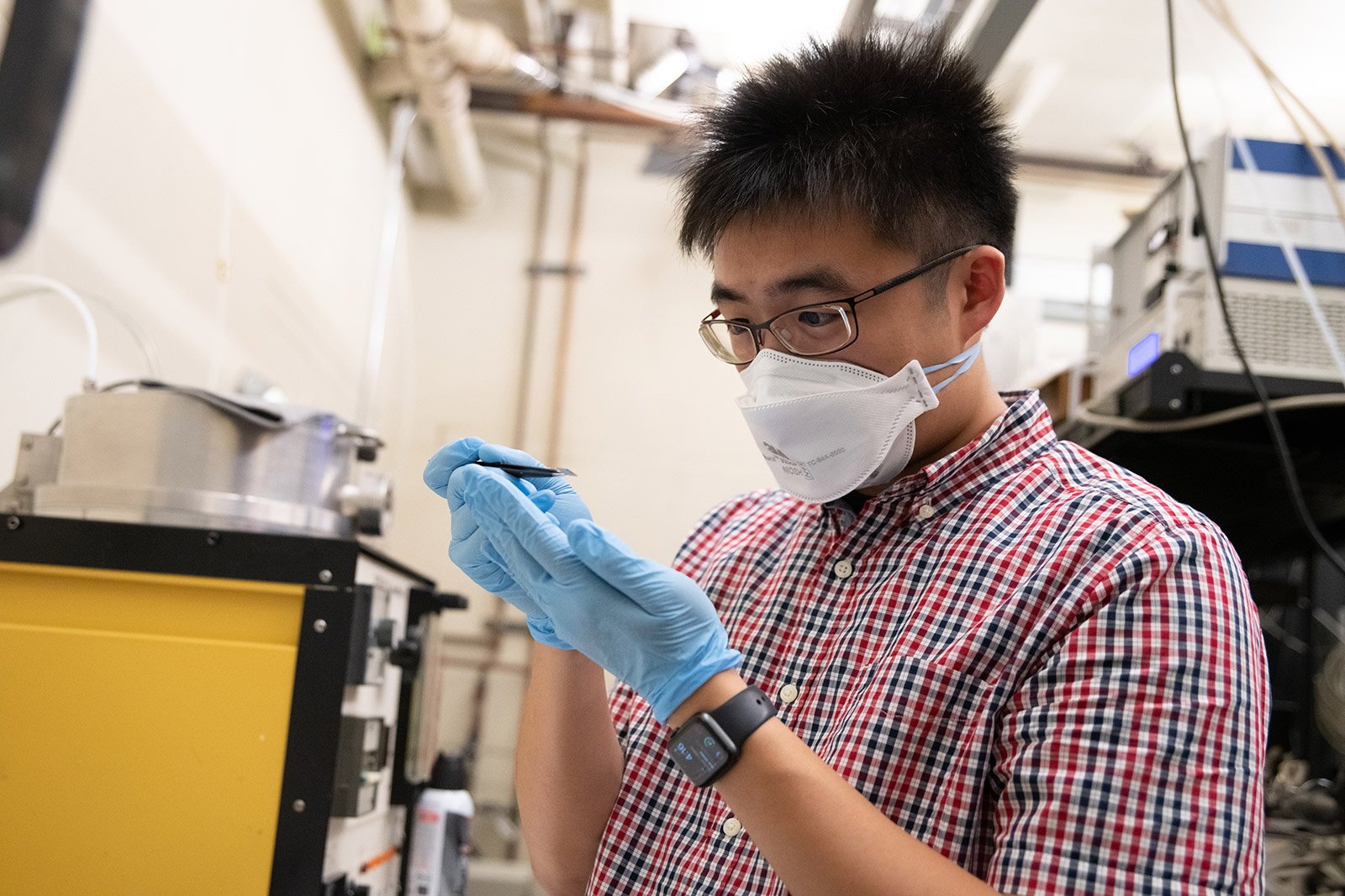
“Flexible and wearable electronics can be made of soft materials like polymers that can't sustain high temperatures,” says Chen-Hsuan (Steve) Lu, a Caltech graduate student and lead author of the three studies. “Our method allows us to grow graphene directly on the substrates at a low temperature, preventing any damage to sensitive materials.”
Yeh adds that their graphene-growth method, which can be scaled up for industrial needs, is compatible with a host of other applications in addition to flexible and wearable electronics.
“Our method is highly compatible with all kinds of substrates, ranging from tiny, nanostructure metals, to semiconducting materials, to even plastics,” she says. “Because we don’t require high temperatures, this method can be used on different substrates for many applications.”

Pink Plasma
The group’s method for growing sheets of graphene is performed in their basement laboratory. A ray of plasma, which glows pink, is used to activate a gas of hydrogen and methane molecules and break them down into smaller fragments.
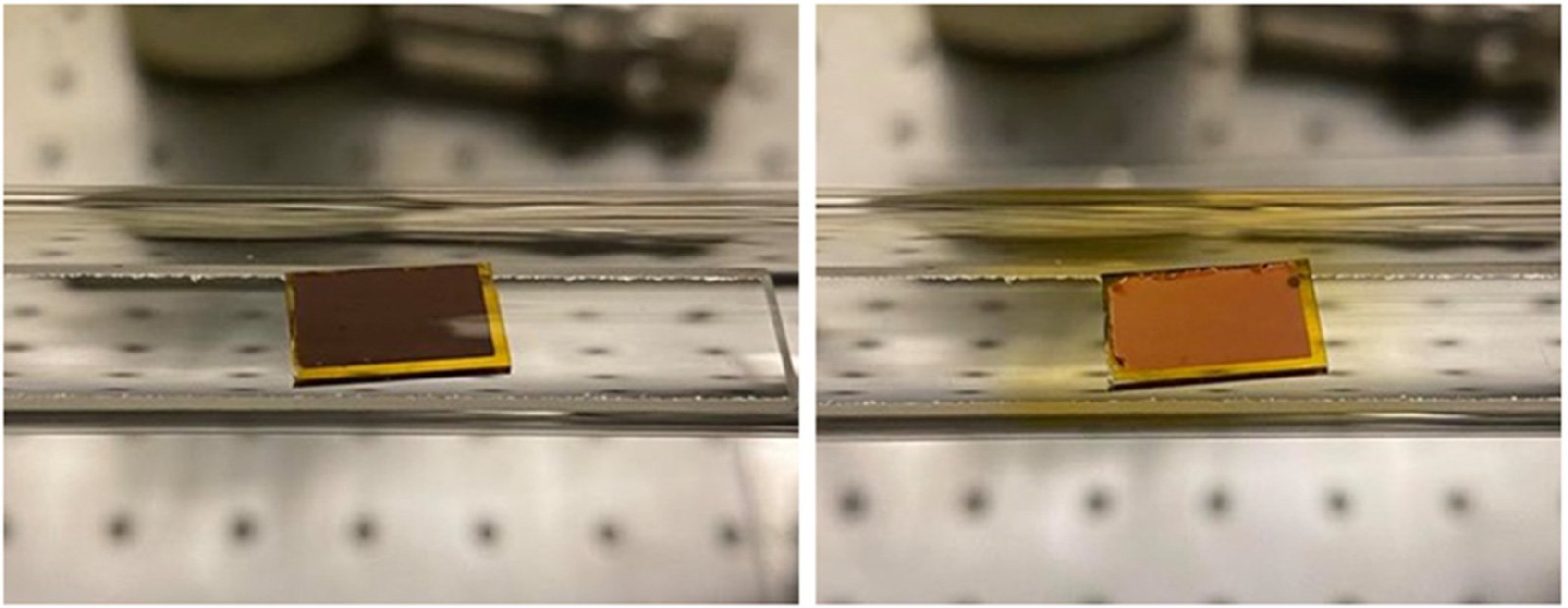
The sample, such as a two-dimensional copper line, is then immersed in the plasma, and the carbon from the gas gets deposited onto the surface in thin sheets that are one atom thick. The final surface with the graphene will appear shinier.
“Because the sample is immersed in the plasma without the need of active heating up to about 1,000 °C by a hot furnace, which is the case with other methods, much lower-temperature growth becomes feasible," Lu says.
For the study testing graphene’s ability to enhance the flexibility of electronics, the team partnered with the materials and chemical research laboratories at Taiwan’s Industrial Technology Research Institute (ITRI). The Caltech team created graphene-coated copper structures that mimic what would be used in flexible electronics and had their partners at ITRI fold them, since the company has enough equipment to repeatedly fold the structures hundreds of thousands of times. “I tried and was not able to stand there and fold the materials this long myself,” Lu jokes.
“The ITRI has been playing an important role in bridging laboratory research to industrial productions in Taiwan over decades,” Yeh explains.
In this same study, the researchers showed that graphene could improve the copper structures’ chemical stability and electrical conductivity, in addition to its structural flexibility. “We put just two atomic layers of graphene on top of these thin copper lines and saw that they were beautifully unchanged after several months,” Yeh says.
The second study tested whether graphene could protect the durability of gold structures used in implantable biosensors. The researchers grew graphene on gold and then exposed the material to saline solutions that mimic sweat. The results showed that the graphene-coated structure remained intact under conditions equivalent to approximately one month at normal human body temperatures, much longer than what is possible with gold alone.
“I wasn’t aware of graphene's full potential when I first started working with it,” Lu says. “But then I realized how it can be used in tandem with other materials for so many applications. My roommate and I were having a boba tea when we realized we could test whether graphene might protect gold from the corrosive effects of sweat.”

Graphene’s Future
While graphene has taken more time to make its way into electronics than first anticipated, its future appears bright, according to the researchers. In addition to the use of graphene in wearable and flexible electronics, Yeh is examining graphene’s potential in everything from energy research and optical communications to environmentally friendly batteries and beyond.
Graphene is also key, she says, to the growing field of nanoelectronics, which aims to create smaller versions of the electronics widely used today. Graphene can be used in combination with silicon to shrink devices down to smaller and smaller sizes.
“Graphene, when combined with other materials, can make our nanotechnologies smaller and faster,” she says. “It leads to lower heat dissipation and energy consumption. In our lab, we use graphene for so many things. It's exciting.”
Source: Caltech, www.caltech.edu.